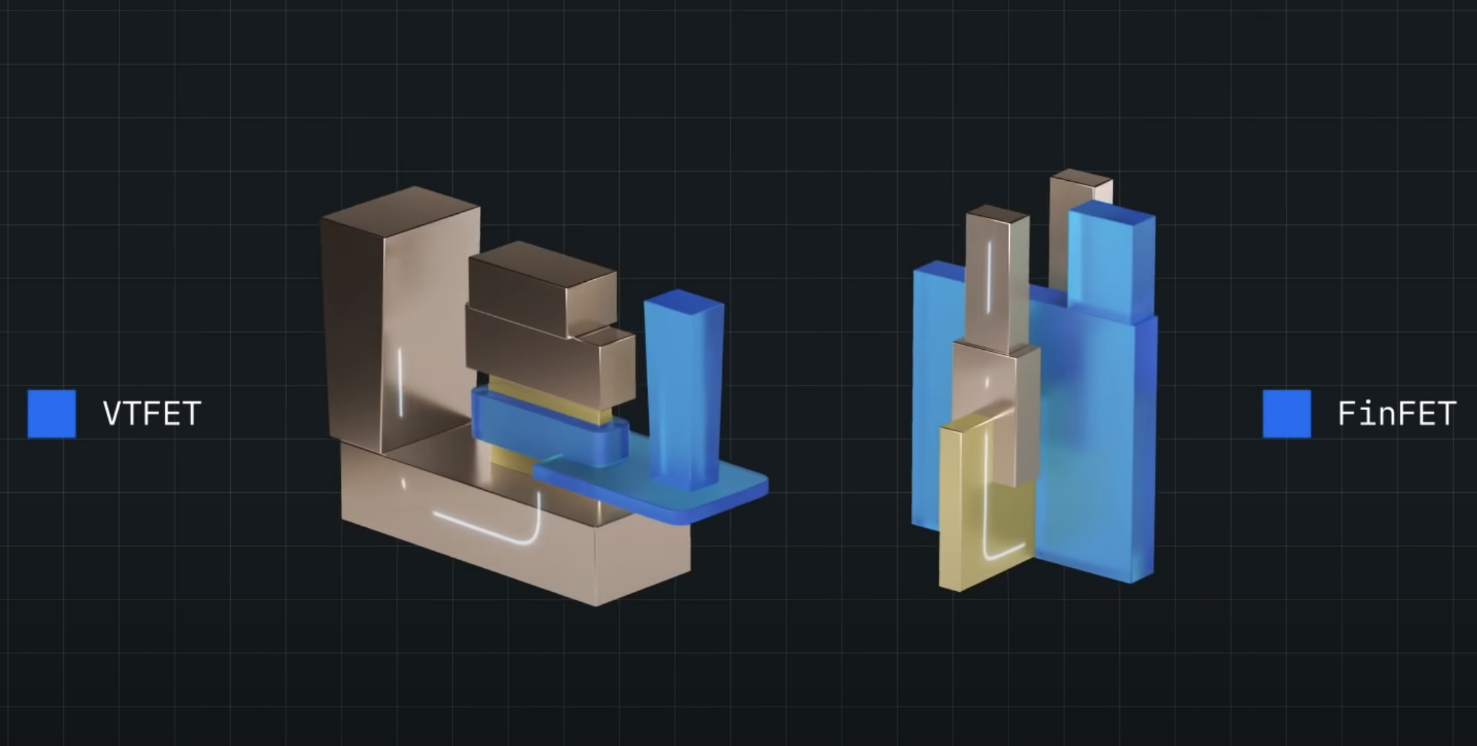
IBM and partner Samsung announced a breakthrough this week, one that could essentially touch every piece of technology ranging from consumer electronics to spacecrafts. Detailed in a video posted to YouTube, a new design for semiconductors would allow chip makers to stack transistors vertically versus the norm of arranging them flat on a semiconductor’s surface.
The current design for this process is called FinFET (Fin Field Effect Transistor), while IBM and Samsung’s new process is called VTFET (Vertical Transport Field Effect Transistors). In plain terms of how this design could affect everyday computing, IBM says that VTFET chips could offer a 2x improvement in performance or an 85% reduction in energy use.
New VTFET Design vs. Old FinFET
Benefits of VTFET
- Potential device architecture that enables semiconductor device scaling to continue beyond nanosheet
- Cell phone batteries that could go over a week without being charged, instead of days
- Energy intensive processes, such as cryptomining operations and data encryption, could require significantly less energy and have a smaller carbon footprint
- Continued expansion of Internet of Things (IoT) and edge devices with lower energy needs, allowing them to operate in more diverse environments like ocean buoys, autonomous vehicles, and spacecraft
For us here at Droid Life, the idea of finally seeing smartphones that can last over a week instead of only a day or two is titillating. Naturally, with this announcement only being made this week, we have a ways to go before we see VTFET implemented into buyable everyday goods for, let alone powering our rocket boots and spaceships. At least we now know what we’re working towards.
For a more detailed look at what’s happening with VTFET, watch the video below.
https://www.youtube.com/watch?v=OF3Zwfu6Ngc&ab_channel=IBMNews
// The Verge